
Pulse modulation has been widely used in radar and various communication systems. But because the power of the modulated signal is minimal, it needs to pass through the power amplifier to obtain enough power and send it to the antenna to radiate out. One standard method is to connect the switch and power amplifier in series to realize pulse modulation. In this traditional circuit, the amplifier and control are separate and independent from each other. The power capacity of the switch is relatively small and can only work at the watt level. When the power is high, the technology of control is not up to the standard, and the isolation of this kind of switch circuit is not enough. When the switch is off, the power amplifier is still working, consumes energy, and generates wide-band noise to interfere with the receiver. The pulse modulation RF amplifier proposed in this paper has no such disadvantages, such as solid isolation, better performance, and higher efficiency.
1. Principle of pulse modulation
In the half-duplex system, pulse modulation is realized using a switch circuit that connects the power amplifier with the switch in series. Suppose the isolation of the control is not enough when receiving the signal. In that case, because the power amplifier is still working when the command is off, it will produce part of the leakage to the low noise amplifier. That is, the broad-band noise will be generated, which will interfere with the reception. Moreover, the power capacity of the switch is small and can only be used for small power signals.
The other is the pulse modulation RF amplifier proposed in this paper. Pulse modulation RF amplifier is a combination of switch and power amplifier, and the amplifier can control its working state.
By changing the bias voltage and the current output, the amplifier can quickly change the working state (working state and non-working state). When applied to the drain or gate of the FET-based amplifier, pulse signal modulation can be realized effectively.
1.1 Gate modulation mode
Gate pulse modulation (GPM), a FET or PHEMT amplifier, can be switched off by clamping the drain current. This requires converting the gate voltage from the fixed operating point (operating state) to the non-functional condition.
1.2 Drain modulation mode
The drain pulse modulation needs to periodically change the drain voltage between the two states: 0V and the voltage VDS required for the amplifier to operate. There are two ways to realize the leakage current according to the size of the drain current needed: one is low power, and the drain current is generally below 100mA. The other is a high power, and the leakage current exceeds typically 100ma
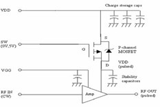
For high power amplifiers, a p-channel MOSFET can be used as a driver to provide a few amps of pulse modulation current, as shown in Figure 1

Figure 1 pulse modulation circuit using driver
Compared with drain modulation, gate modulation has two disadvantages. Usually, people choose drain modulation. First of all, many amplifiers work around the VDS value, which limits the static operating point very low. When you put the gate in the cut-off
At the same time, VDS is increased, and the result is likely to enter the breakdown region, which is more difficult to achieve.
Secondly, there is little difference between the two voltage values, and the gate voltage is more strict than the drain voltage in practical operation.
Drain modulation is also used in this paper.

2. Design of control circuit
The control circuit makes use of the feature that p-channel MOSFET can be used as a switch. The grid voltage VG controls the switch state. The main advantage of using FET as a microwave switch is that it can simplify the bias network, reduce driving power consumption, have broadband characteristics and considerable power capacity, and provide high switching speed.
The application of p-channel MOSFET is inferior to that of n-channel MOSFET in other aspects, but from its output characteristics, it is more suitable for the control circuit.
We use ADS software to simulate the control effect of MOSFET in the time domain. Source input (i.e., adding DC voltage), gate control signal, and drain output. The results show that the control effect of the tube is good, and the line works linearly when it is on, and the output voltage is equal to the input voltage.
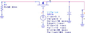
The design of the whole control circuit is shown in Figure 2. V2 is the output terminal connected with the amplifier's drain bias voltage input terminal. For the convenience of simulation, we terminate a 50ohm resistor here.
Figure 2 circuit diagram of control circuit